![]()
![]()
An old ZX81 PCB that you don't use anymore could certainly be used as a mainboard for a ZX96 system, however this has several disadvantages. For example, an additional Poke Board must be built into the system. Besides that, someone who is familiar with electronics will in most cases want to do without the internal ZX81 modulator (which could be soldered back into the system on the AT Keyboard Interface in case someone would still want to use it!). So the ZX96 Mainboard is in essense a ZX81 without a tv modulator, with an integrated Poke Board instead.
The ZX96 Mainboard PCB can NOT be built back into the original ZX81 case! Besides this, the EAR and MIC connectors and the voltage regulator are not present anymore on the ZX96 Mainboard. The PCB does NOT have an edge connector either, instead of that a 50pin connector is used to connect the ZX96 Mainboard to the Bus Driver Board. This assembly (ZX96 Mainboard, Giant Board, Driver Board) merges into a compact module that can be inserted into a (larger) case.
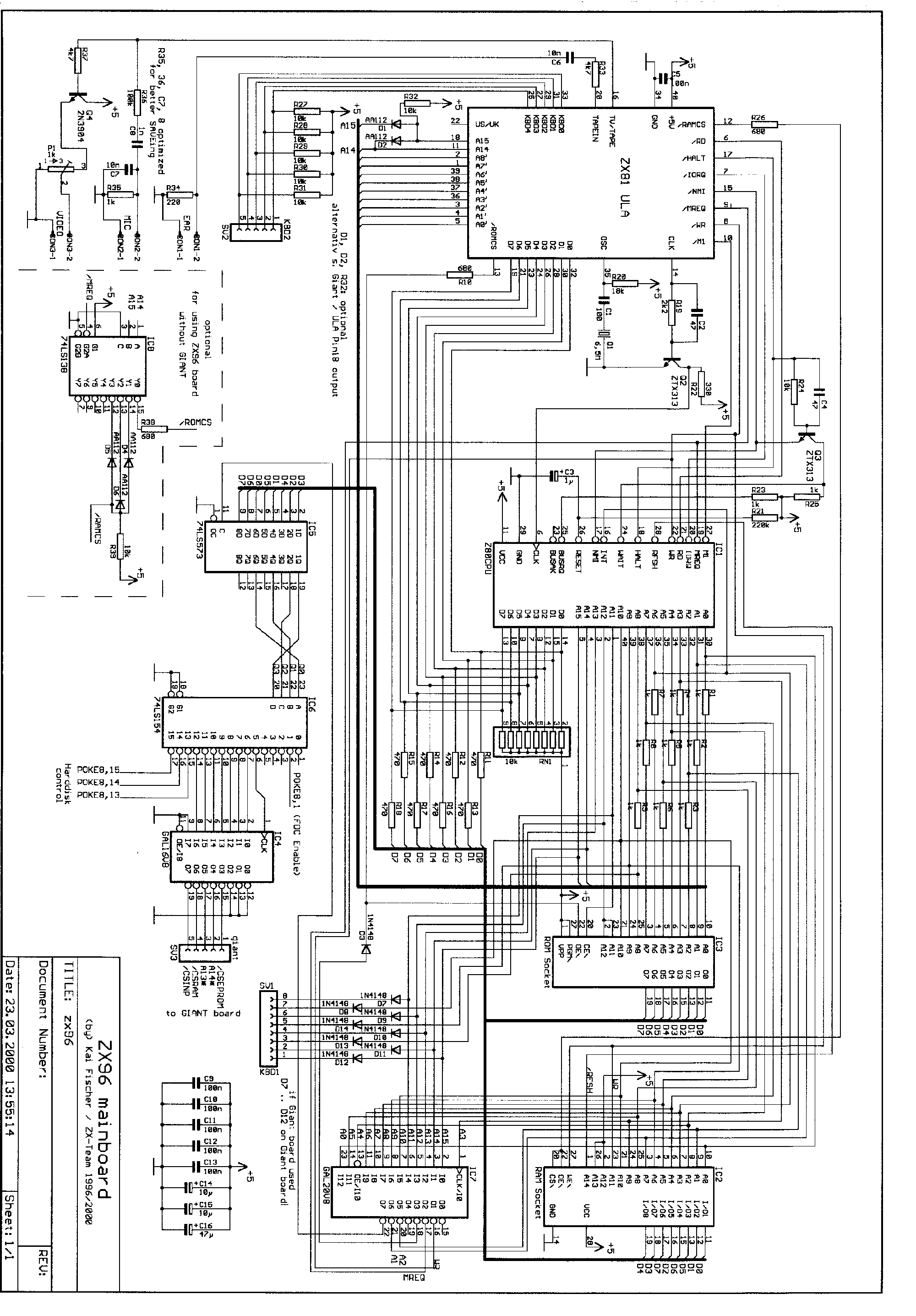
The circuits on the ZX96 Mainboard are identical to the ZX81's circuits, with one exception, in order to achieve a stronger signal level, the MIC output has been slightly modified. The video output is nothing special, except that the video signal level is adjustable. For the ZX81 there have been two ULA chips in production: the 184 ULA and the 210 ULA. As it turned out, with the 184 ULA the TV picture was not so good(rather dark and with poor contrast) as with the 210 ULA. Of course, the simple solution would be to make sure you use a 210 ULA. A slightly more difficult solution is to build a different video output circuit. Occasionally the video inverter on the AT Keyboard Interface can already produce a noticable improvement.
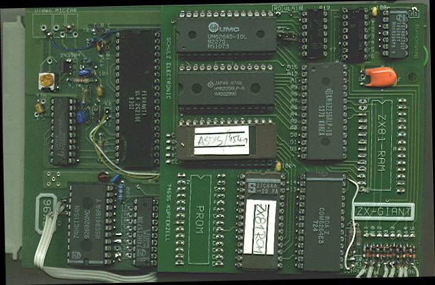
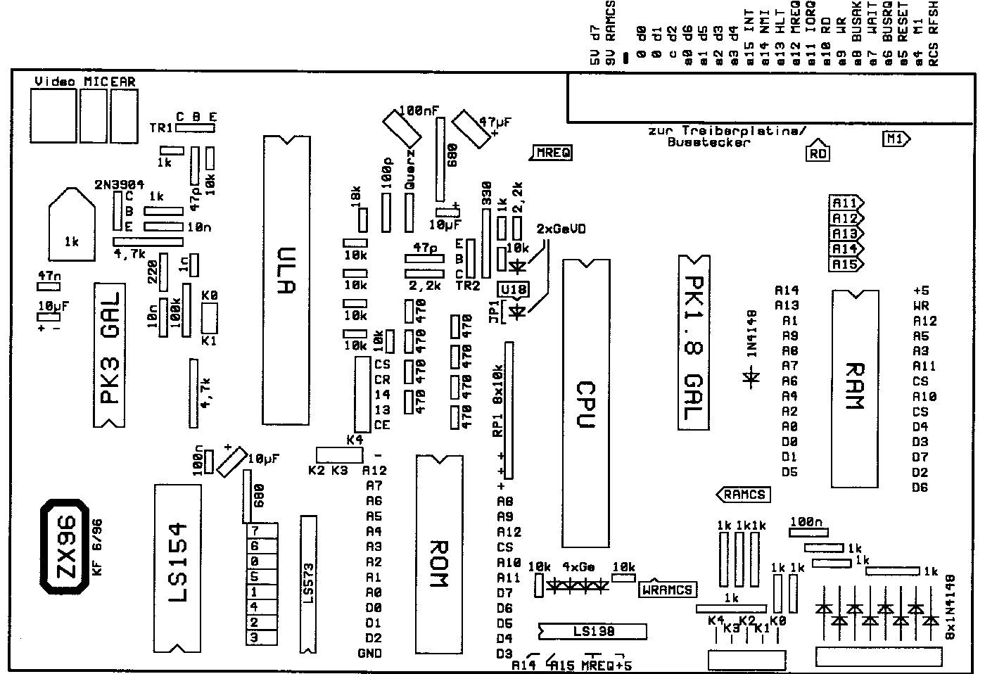
The placement order of the ICs is identical to the ZX81, since the Giant Board needs to be able to fit perfectly on both PCBs.
For the Giant PCB there are several solutions to plug it onto the ZX96 Mainboard. If you use regular IC sockets to build the ZX96, the Giant has to be built with more delicate round pin row connectors. The distance between the boards will be very short with this method, which means that the component pins on the bottom of the Giant PCB in the area of the CPU underneath on the Mainboard have to be carefully filed off to make them as short as possible. You will have considerably more space between the boards when you use the thicker and longer square pin connectors. However, these have the disadvantage that you can not use the female connectors on the ZX96 Mainboard as IC sockets.(for testing purposes) Three signals have to be connected to the Giant Board by additional wires: /RD, /M1 and ULA-Pin18. The soldering points are respectively marked on both PCBs.
On the PCB there is a via(top to bottom layer connection) under the LS573 IC which connects ROMCS to GND. Please do not forget to drill this via out!
Differences in the component list, in case no Giant Board is used: (compare the schematic)
| Schematic | 179k |
| Parts list | 1k |
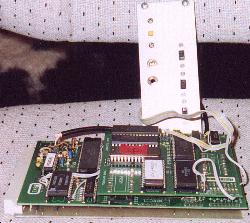
| Photo of PCB with Giant plugged in | 63k |
| Component placement diagram | 40k |
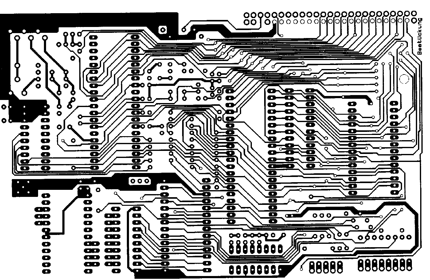
| PCB Layout component side | 52k |
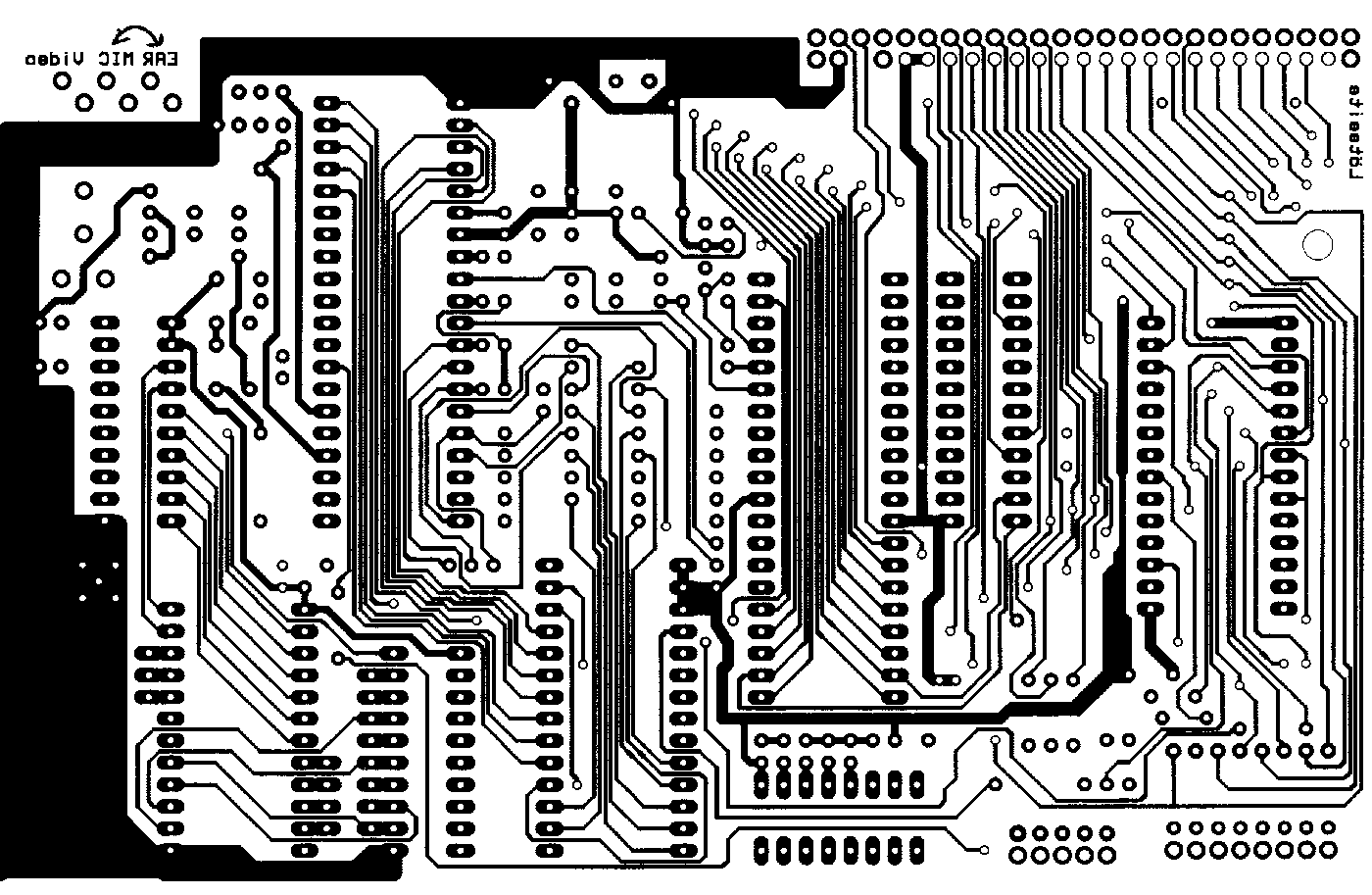
| PCB Layout solder side | 69k |
| Schematic in EAGLE-Format | 26k (zip) |
| www.cadsoft.de | EAGLE Freeware (about 4MB) |
The layouts are only provided for informative purposes
and certainly not suitable for etching and building! The PCB was designed
with an old EASYPC. If anyone wants to make a new layout using the Eagle
schematic provided here, please let me know well in advance!!
last updated Mar/00
